
Rapid PCB prototyping is a process that allows for the quick and efficient creation of printed circuit board (PCB) prototypes. Our Mefron’s technology has revolutionized the way that PCBs are designed and manufactured, enabling designers and engineers to quickly and easily create functional prototypes of their designs.
The process of creating a PCB prototype involved designing the board on a computer using specialized software and then sending the design to a manufacturer for production. This process could take weeks, and often required multiple iterations and revisions before a final design was approved.
This can be done using specialized software and 3D printing technology, which can produce a physical prototype of the PCB in a matter of hours. This allows designers and engineers to quickly test and iterate on their designs, without having to wait for the production process to be completed.
One of the key advantages of Rapid PCB prototyping is the ability to quickly and easily make changes to the design of the PCB. With traditional manufacturing processes, making changes to a PCB design could be time-consuming and costly. With PCB prototyping, however, changes can be made quickly and easily, allowing designers and engineers to easily test and iterate on their designs.
Another advantage of PCB prototyping is the ability to create complex and intricate designs. Traditional manufacturing processes often have limitations when it comes to creating complex PCBs. But with rapid prototyping, designers and engineers can create PCBs with a wide range of features and capabilities.
Types of PCB prototyping
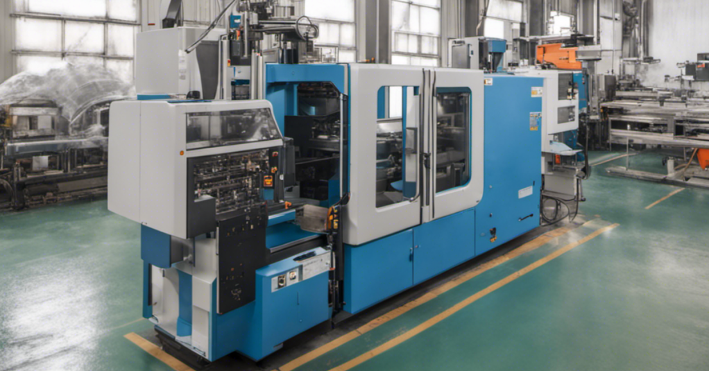
There are several different types of rapid PCB prototyping, each with its own unique set of advantages and disadvantages. Some of the most common methods of rapid PCB prototyping include 3D printing, laser cutting, and milling. Besides the manufacturing process involved, prototyping involves different levels of fidelity.
The Fidelity of types refers to the level of closeness to the actual design. The OEM should have clarity about the functionality, size, shape, and all specific requirements of the prototype. The manufacturer will accommodate components and route accordingly.
Low fidelity:
It means the designers need a basic prototype that just implies the basic functions such as size, shape, and weight that exactly replicate the design. The quick turn-around prototype is mostly for mock testing.
High Fidelity
The circuit board works exactly like the actual PCB, designers use it for testing all the parameters of the design. Designers can connect the PCB with the device and check the working and decide on the further development process.
Real PCB prototype:
It will be the replica of the actual PCB. Designers need such PCB prototypes to overview the capability of EMS services and check the working condition of their design. PCB allows designers and engineers to test out their designs and make any necessary modifications before moving on to the final version. It also allows designers to change the requirements live while manufacturing is underway.
Advantages of Rapid PCB prototyping
PCB prototyping is a valuable tool that offers a range of benefits, including the ability to quickly and easily test out new designs, make modifications to the design in real-time, and create multiple prototypes at a low cost. By using prototyping, you can save time and money, and ensure that your final design is thoroughly tested and ready for production. Here are some potential advantages of PCB prototyping that you could mention in a technical blog:
- Fast turnaround: Prototyping allows you to quickly and easily test out new designs, which can save a lot of time and effort compared to traditional fabrication methods.
- Real-time modification: With prototyping, you can make modifications to your design in real-time, which allows for greater flexibility and faster iteration.
- Low cost: Prototyping allows you to create multiple prototypes at a relatively low cost, which is particularly useful for early-stage product development.
- Thorough testing: Prototyping allows for thorough testing and debugging of your design before it is finalized, which can save time and money in the long run.
- Small quantities: Prototyping allows you to produce small quantities of PCBs, which is useful for testing and early-stage product development.
- Customization: Prototyping allows you to create custom boards for specific applications, which can be particularly useful for niche products or specialized applications.
Conclusion
In conclusion, rapid PCB prototyping is a revolutionary technology that has greatly improved the design and manufacturing process for printed circuit boards. Mefron Technologies are allowing to designers and engineers to quickly and easily create functional prototypes of their designs and makes it possible to easily make changes and improvements to the design. This technology has greatly improved the speed and efficiency of the PCB design and manufacturing process and will continue to be a valuable tool for designers and engineers in the future.


Leave a comment